

The impact of high-speed PCB design
With the continuous and increasing demand for electronic devices, designers are persistently finding ways to enhance performance and put out the best electronic product in the market.
Simultaneously, the designers need to account for the possible effects of high-speed signals in a PCB layout, considering that increasing clock frequencies and decreasing rise times may result in fluctuating signal or signal integrity issues.
You must use higher frequencies to overcome this issue. Hence, higher frequencies, ranging from 50MHz to 3GHz, have become a staple in designing PCBs.
Implementing effective high-speed PCB design is vital to meet and support real-world demands.
However, there are three main hurdles to overcome in dealing with high-frequency boards. These are:
- Signal integrity
- EMI/EMC
- Dielectric loss.
Since signal transmission issues are remarkable when a PCB works with high-speed signals, an outstanding high-speed PCB incorporates different components and routing while deflecting signal integrity issues simultaneously.
Here at QuantumCAD, we’re experts in a range of custom PCB design processes – including high-speed PCB design.
Using our expertise in the field, this article will explain crucial factors to consider during the high-speed PCB design process, including the impact of wiring topology, taking care of signal integrity, and more.
What is a high-speed signal in a PCB?
Signal frequencies ranging between 50MHz and 3GHz are considered high-speed signals, such as clock signals.
In principle, a clock signal is ideally a square wave. Yet, the “LOW” level cannot instantaneously become a “HIGH” level or contrariwise.
Rather, the clock signal must adhere to a specific rise and fall time because of what appears to be a trapezoid in the time domain. Notably, the amplitude of the higher frequency harmonics of the clock signal is contingent on the rise and fall time. Specifically, if the rise time is longer, then the magnitude of the frequency harmonics will be shorter.
The impact of wiring topology on signal integrity
When signals transmit along the line on a high-speed PCB, signal integrity issues can occur.
The impact of wiring topology on signal integrity gets recognised in the fluctuating and inconsistent signal arrival times at each node. Plus, the timing at which the reflected signals arrive at a certain node is also irregular.
These inconsistencies result in the decline of signal integrity.
Generally, the Star Topology is used to prevent signal integrity issues. With the star topology, you can manipulate the signal transmission and reflection delay by controlling several equivalent lengths to improve signal quality.
Before using a specific topology, it’s imperative to consider the signal topology node conditions, the working principle executed, and the wiring difficulty.
Different buffers pose different effects on signal reflection. This means that, although generally helpful, the star topology may not solve certain devices’ signal delays, such as the digital address bus connection to FLASH and SDRAM.
On the other hand, on a daisy chain topology, the signal is generally communicated between the DSP and the SDRAM, ensuring the signal’s quality.
FLASH does not have a high loading rate, meaning that, in high-speed simulations, paying attention to the waveform at the FLASH is unnecessary as long as the waveform at the node, where the high-speed signal is transmitted, works efficiently.
Additionally, routing is essentially tricky, but unlike the daisy chain topology, having a massive sum of data address signals in a star topology makes routing extra challenging.
When do we need to take care of signal integrity in high-speed PCB design?
In principle, on a PCB, a signal should travel unimpaired and undamaged from a source (Tx) to a load (Rx), but this is not always the case.
More often than not, the signal gets to the load with a few losses, either by impedance mismatch, crosstalk, attenuation, reflection, or switching issues.
1 – Signal integrity
Signal Integrity (SI) is the measure of signal distortions and fluctuations in the high-frequency domain. Signal integrity enables the generation of practical solutions to predict and understand the critical issues revolving around the high-frequency field.
Rather than simple wires, high-speed PCB design requires traces to visualize as transmission lines.
Once the highest operating frequency in the design gets identified, it’s easier to target the pathways used as transmission lines for better signal transmission. These transmission lines must undergo digital and analog analyses to ensure functionality.
2 – PCB substrate
Another factor that you must consider in high-speed PCB design is the substrate material to be used.
Each PCB substrate has a unique dielectric constant (εr) value. This value determines the length at which signal traces can pass as transmission lines. With this available data, the PCB designers can manipulate and prevent signal integrity threats.
Specifically, with the dielectric constant (εr) value, designers can examine and evaluate the velocity (Vp) at which the signal flows and propagation delay (TPD).
Even more so, it’s crucial to take into account how insertion loss increases with signal frequency. The insertion loss (per inch) gets measured for FR-4 (glass epoxy) and high-frequency Rogers RO4350B material.
In sum, higher insertion loss may lead to more attenuation.
3 – How to suppress electromagnetic interference
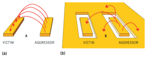
Since the PCB is the source of Electromagnetic Interference (EMI), the high-speed PCB design is directly related to the Electromagnetic Compatibility (EMC) of various electronic products.
Giving enough focus on EMI/EMC shortens product development cycles and accelerates time-to-market rates.
Considering the EMC, it is important to consider its three key elements:
- The source of radiation
- The route of transmission
- The victim.
The propagation route gets sectioned off into space radiation propagation and cable conduction.
It’s imperative to look at how it spreads first to suppress the harmonics. Power Supply decoupling, together with the necessary matching and shielding, is required to address conduction propagation.
One way to solve the problem of EMC radiation through conduction is by Filtering.
Additionally, you can consider the problem from the source of interference and the victim. For interference sources, consider using an oscilloscope. Using this, check whether the rising edge of the signal is too fast or whether there is reflection or overshoot, undershoot, or ringing. If there are any, consider matching.
Additionally, avoid using the subharmonic, 50% duty cycle signal that only demands more high-frequency components.
Finally, in terms of victims, consider measures such as land acquisition to address the problem.
Conclusion
With the continuous progression and advancement in our modern world, High-Speed PCB design is necessary and essential to keep abreast with our developing times.
Contact us
Is your business in need of expert high-speed PCB design services to keep up with the increasing product demand?
QuantumCAD can help.
With over 25 years under our belt in designing custom PCBs, numerous qualified PCB designers, and experience in working with some of the biggest brands, including Jaguar and Ericsson, we can deliver a custom high-speed PCB that suits your needs.