

High power PCBs
High-power PCBs are printed circuit boards that are designed to handle higher currents and withstand high temperatures.
There is now a growing demand for high-power PCBs. This is because modern and up-to-date electronic devices need to operate at faster speeds due to their more advanced components that need to combat current needs and complexities.
This blog is going to discuss what high-power PCBs are, what they’re used for, and the challenges in designing them.
What are high-power PCBs?
As previously mentioned, high-power PCBs are those that are designed to withstand higher currents and temperatures.
They are typically made from copper because copper has low resistivity and therefore makes for an excellent conductor. Copper has been used as an electrical conductor since the early 1800s, and due to its high level of electrical conductivity, it’s still the first choice for any electrical connector.
What are the differences between high-power and regular PCBs?
- The material choice – Because high-power PCBs experience extra stresses on its thermal conductivity, the material choice will differ depending on whether you’re designing regular or high-power PCBs.
- The coefficient of thermal expansion – For high-power PCBs, this must be selected in a way whereby the expansion or contraction of the material caused by the additional high-power doesn’t cause mechanical stress on the PCB.
- High-power PCB material must also have low loss, as a high-loss PCB generates more heat.
In the custom PCB design process, there are extra considerations that have to be made when designing high-power PCBs over regular PCBs. See this list of considerations further down.
How many amps can a PCB handle?
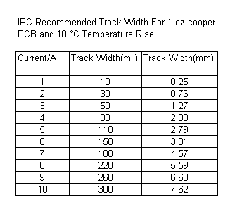
There are numerous manufacturing possibilities for a PCB, including copper thickness, number of layers, the material used, and more. However there are general guidelines in the public domain surrounding track widths to carry specific currents to take advice from.
The chart below shows an IPC chart offering simple information on 1oz copper.
Designing high-power PCBs
PCBs that are used for RF applications, amplifiers or power conversion circuits will need careful consideration in terms of key design elements.
These include thermal conductivity (TC), thermal expansion (CTE) and material losses. Calculations at the start of the project are critical in choice of PCB topology and materials.
When designing high-power PCBs, both thermal design and heat dissipation must be optimised, which is a significant challenge for designers.
In addition, designing high-power PCBs require further considerations than when designing regular PCBs because both thermal design and heat dissipation must be optimised, which is a significant challenge for designers.
These additional considerations are:
- Safety – Heat dissipation and short circuits are both potential safety hazards that need to be considered in the design process.
- Planning the layout – When designing high-power PCBs, you need to allow sufficient space between the components for copper pours, increased via sizes and trace widths.
- Trace widths – You should use a trace width calculator to ensure the high-power PCB has the capacity to carry the sufficient current required.
- Copper pours – Use copper pours wherever possible to aid heat dissipation.
- Double up on layers – By doubling up on layers of copper pours stitched together with vias, you will achieve greater heat dissipation.
- Thermal reliefs or Solid floods – Use thermal reliefs on all non-power nets. However, high-power nets are better with solid copper to pads. Note that these may need to be hand soldered.
- Thick PCBs – Thick PCBs create more space which allows heat to dissipate more effectively, resulting in the potential to reduce the overall board size.
- Materials – Remember to select the appropriate material for your application. As mentioned FR4 is the most commonly used material in PCB manufacturing, but if a high-power PCB has requirements that can not be achieved using FR4, materials such as Rogers substrates, pedestal PCB, insulated metal substrates (IMS) and copper INVAR.
Contact us
With the multiple things that need to be taken into account when designing high-power PCBs, it’s essential that you know exactly what you’re doing.
Another option is to use an expert, like us, to design your high-power PCB for you.
With over 25 years of experience, our specialist team has the skills to design your high-power PCB.
Simply get in touch with us to speak to one of our PCB experts and start your project today.