

Common PCB Design Mistakes
With PCB Design re-spins costing in excess of £15,000 (not taking into account lost opportunity) eliminating unnecessary mistakes is an important company objective. Read on to find out more about ways to avoid wasting precious time and money, and to streamline your work process.
Use Valid Parts
Before even starting PCB design you first need to consider, are you using valid parts in your design?
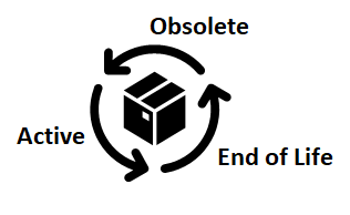
- Availability? If not, these should be designed out to avoid timescale and budget increases.
- Recommended for use? Manufacturers are discontinuing or replacing parts continuously. Design out these parts.
- End-of-life? Just because you used a part on your last PCB design doesn’t mean you should use it again.
- Check before you create: When deciding on a part, do you check its status before adding it to your CAD library?
There are solutions that allow you to load your BOM and check the validity of your parts, which could end up saving you a re-spin.
Footprint errors
- Your ECAD library: This must be verified, as your ECAD library forms the foundations of your products. Please do not take short cuts with your ECAD library, and don’t commit the cardinal sin of every engineer having their own library. If your foundations are unstable you will pay the price later in the product lifecycle, which will end up costing much more to rectify down the line.

Communication
- Can you build it? Don’t design in isolation. Communicate with your PCB manufacturer and PCB assembler: they will be more than happy to work with you. Your CAD system will allow you to design anything if you define unrealistic rules. Your design may look fantastic but if it can’t be made, you’ll be wasting your time.
- Fail to plan, plan to fail: Resist the temptation to just dive into laying out your PCB. Take a step back and review the challenges you are facing. How do the functional blocks of the schematic interrelate and how could they fit onto the board? Once defined, review with the engineer before you have to make wholesale changes. Then and only then look at the detail.
- Review and then review again: Define your milestones and perform smaller reviews regularly. Catch those issues as early as possible before they have a major impact on your PCB design.

- The late design change: You have just finished, you have created all the manufacturing files, and can breathe a big sigh of relief. It’s nearly the end of the day and then it happens: the late design change and the pressure is on. Make sure you understand the impact of the change, and don’t take any short cuts. ‘Less haste, more speed’!
We can eliminate many issues just by changing the process in which we design. This is the way we work at Quantum CAD to make sure our work is as efficient as possible. In our next blog we will be taking a look at Common PCB Design Mistakes of the actual PCB design itself, check back soon to read all about it.
Interested in discovering how Quantum CAD can help your business?